The process
I started with hand-wired LEDs in a printed case. Making more meant designing a PCB, revising the case around it, and making tools to help with both.
Software jigs
I had no idea what a jig was when I started. This happened to overlap with my carpentry class at CCSF, and I realized the idea was the same: make a tool bespoke to a task that helps you do it more accurately and repeatedly.
I used software jigs a lot: small tools that made it easier for me and AI to work on the same problem. AI could help with the code and CAD, but it still needed feedback. Sometimes I could see what was wrong much more easily than I could describe it.
The lid was a good example. Its openings had to line up with the LEDs and button underneath. An editor put circles over a photo of the beacon; I could drag them into place, nudge them, or adjust their sizes. The tool then exported those corrections as coordinates for the CAD model.
That gave us a useful loop: AI makes a first pass, I adjust what I can judge by eye, and the next version uses those exact changes.
- SoftwareFirst passDetect the features in a photo.
- MeVisual correctionMove and resize the circles.
- The jigBack to the modelExport the corrected coordinates.
Other jigs handled checks that would be tedious to repeat by hand. For the PCB case, a script reads the board outline, mounting holes, button opening, and ESP32 position directly from KiCad. It checks the case against those measurements, including room for the solder joints underneath.
Decorating the lid
I started with the layout: where the LEDs and button needed to come through the lid. Then I used AI image generation to explore pattern ideas around those openings, with inspiration from mycelium, lily pads, and topographic maps.
Once I had a direction, I asked Codex to turn the pattern into raised geometry by extruding it to a chosen height. I kept the decoration as a separate STL and placed it on the lid, so I could work on the pattern separately from the lid itself.
PCB v2
Once I had a working hand-wired prototype, I designed a custom board and had PCBs manufactured in China. The next version addresses both the electronics and the fit of the parts.
The ESP32 headers were too tight. The original footprint had 24.75 mm between rows; the revised one uses 25.4 mm, measured from the centers of the pins. The difference is only 0.65 mm, but it was enough to make the earlier fit bind.
V2 also adds a level shifter between the ESP32 and the LEDs. It translates the controller’s 3.3 V data signals to 5 V for the two LED circuits. The series resistors sit next to its outputs, and a bypass capacitor sits beside the chip.
The layout had to work inside a circular case. I moved the ESP32 inward so its corners sit within the board edge, kept the button near the center, and put the mounting holes in the lower half of the board. Those positions also determine where the case needs supports and openings.
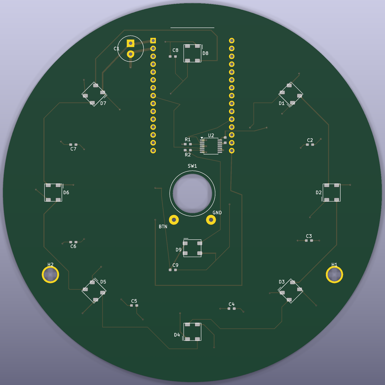
The v2 manufacturing files split the work between factory assembly and hand soldering. The factory assembly list includes the LEDs, resistors, small capacitors, and level shifter. The ESP32 headers, bulk capacitor, and button wires are left for me to solder.
Getting the case to fit
The newer case follows the PCB geometry: supports under the board, clearance around the ESP32, and openings for the button and USB cable. The fit checks use the board file so that a change in the layout can be checked against the enclosure.
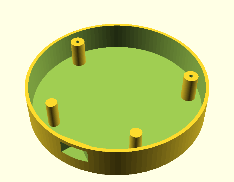
The v2 board and this case have passed the file-based checks. Their fit together still needs confirming with the actual parts, especially the USB cable body, button terminals, and space under the board.
Small lessons from building
I learned to 3D print smaller test parts before committing to a whole enclosure. Printing just the area I wanted to check made it quicker to try a fit, adjust it, and try again, with less time and filament spent on each iteration.
Another lesson: a USB cable can power a board without carrying data. Some cables are charge-only: the power connections work, but the data wires are missing or disconnected. A matching connector and a powered-up board don’t tell me whether the cable can transfer data, and the difference isn’t always visible. Uploading firmware over USB needs a data-capable cable.
Keeping the lights up to date
The button and app send status changes to a Cloudflare Worker. It saves the change in D1, works out what each person is allowed to see, and sends the resulting display to their beacon.
- Button or appSend a status change.
- Worker + D1Save it and apply sharing permissions.
- ESP32 + LEDsReceive the update and change the lights.
Updates arrive over MQTT. The broker keeps the latest display so a beacon can pick it up when it reconnects. The device also checks over HTTP in case it missed something: every 30 seconds when messaging is unhealthy, or every two minutes when it’s working.
Both routes use the same parser. The firmware ignores older updates so a delayed message won’t overwrite a newer status.
What I’m trying next
Now that friends have beacons, I’m finding that it works better in small friend clusters. It’s already led to some hangouts, and I’m watching where people get stuck.
One friend asked for an invite feature for people using just the phone app, without a beacon. That’s one direction I’m considering next.
← Back to the overview